Login With Mobile OTP


Top Rated Material Testing Lab in Chennai | Kiyo R&D Center & Laboratory

Top Rated Material Testing Lab in Chennai | Kiyo R&D Center & Laboratory

Top Rated Material Testing Lab in Chennai

Reliable Testing Lab in Chennai for Plastics, Metals & Materials

Top Rated Material Testing Lab

Choosing the right testing lab is not a small decision. One wrong result can affect product approval, customer confidence, production quality, and business reputation. That is why industries look for a top rated material testing lab in Chennai – Kiyo R&D Center & Laboratory when they need reliable testing support.

Kiyo R&D Center & Laboratory provides material testing and analysis services for plastics, polymers, rubber, metals, coatings, composites, packaging materials, automotive components, and industrial products. Our focus is simple: accurate testing, clear reporting, and practical technical support for better client decisions.

Top Rated Material Testing Lab in Chennai | Kiyo R&D Center & Laboratory

What Makes a Material Testing Lab Top Rated?

A top rated lab is not defined by claims alone. It is defined by technical capability, reliable results, professional communication, and client trust. A good lab must understand the material, the test method, the standard, and the purpose of the report.

When clients choose a top rated material testing lab in Chennai – Kiyo R&D Center & Laboratory, they expect correct testing, proper sample handling, method clarity, and dependable reports that can support quality control, customer submission, R&D, and failure analysis.

Testing Services at Kiyo R&D Center & Laboratory

Kiyo R&D Center & Laboratory supports a wide range of testing services for industries across Chennai, Oragadam, and nearby manufacturing regions.

Common services include:

  • Mechanical testing such as tensile, flexural, impact, compression, and hardness
  • Plastic and polymer testing as per ASTM, ISO, IS, and customer specifications
  • Thermal analysis such as TGA and DSC
  • Chemical identification using FTIR, Raman, and related methods
  • SEM and EDAX analysis for surface and elemental investigation
  • Rubber, coating, corrosion, and durability testing
  • Failure analysis and product validation support

Why Accuracy Matters More Than Just Fast Reports

Fast reports are useful, but wrong reports are dangerous. A rushed test result can lead to wrong material approval, rejected products, repeated failures, and unnecessary rework. A professional lab balances turnaround time with proper testing discipline.

At Kiyo R&D Center & Laboratory, the goal is not just to issue a report. The goal is to provide useful, technically reliable data that helps clients make better decisions.

Industries That Need Material Testing Support

Material testing is required across industries where performance, safety, durability, and compliance matter.

Industries commonly served include:

  • Automotive and engineering component manufacturers
  • Plastic and polymer product manufacturers
  • Electrical and electronics industries
  • Rubber and elastomer product manufacturers
  • Paint, coating, and corrosion protection companies
  • Medical device and packaging manufacturers
  • R&D teams, consultants, students, and quality departments

Why Choose Kiyo R&D Center & Laboratory?

Clients need more than a testing machine. They need a lab that can understand requirements, guide test selection, handle samples properly, and provide clear reports.

Key advantages:
  • Wide material testing and analysis capability
  • Support for plastics, metals, rubber, coatings, composites, and industrial products
  • Experienced technical team
  • Professional reporting for customer, R&D, audit, and quality documentation
  • Practical support for urgent testing, validation, and failure investigation
Top Rated Material Testing Lab in Chennai | Kiyo R&D Center & Laboratory

Speak to an expert

A testing lab should not be selected only by price or convenience. The quality of the report affects the quality of your decision. If the testing is weak, your approval, production, and customer confidence are at risk.

If you are looking for a top rated material testing lab in Chennai – Kiyo R&D Center & Laboratory, our team can support your requirements with reliable testing, technical clarity, and professional reporting.

FAQ

Why should I choose a top rated material testing lab instead of a basic local lab?

A top rated material testing lab provides better technical support, correct method selection, reliable testing, calibrated equipment handling, and professional reports. A basic lab may only provide numbers without useful interpretation.

Can Kiyo R&D Center & Laboratory help with urgent material testing requirements?

Yes. Kiyo R&D Center & Laboratory can support urgent testing requirements depending on sample availability, test method, instrument schedule, and reporting scope. Sharing full details early helps speed up the process.

Does the lab provide reports for customer submission and audits?

Yes. Test reports can be used for customer submission, supplier approval, internal quality control, R&D comparison, audit documentation, and failure investigation depending on the test scope.

What details should I provide before asking for a quotation?

For a faster quotation, share the material type, test name, required standard, number of samples, sample dimensions, application, urgency, and whether the report is needed for internal use, customer submission, or audit purpose.

Why do clients trust Kiyo R&D Center & Laboratory for material testing?

Clients trust Kiyo R&D Center & Laboratory because the lab provides wide testing capability, technical guidance, reliable reports, and practical support for quality control, product validation, R&D, and failure investigation.

Thermal Conductivity Analysis Services in Oragadam | Kiyo R&D Center & Laboratory

Thermal Conductivity Analysis Services in Oragadam | Kiyo R&D Center & Laboratory

Thermal Conductivity Analysis Services in Oragadam

Best Thermal Conductivity Testing Services for Materials – Kiyo R&D Lab

Thermal Conductivity Analysis Services

Heat management is a serious performance factor in modern materials. A product may look strong and well-designed, but if it cannot control heat properly, it can fail during actual use. This is why thermal conductivity analysis services in Oragadam – Kiyo R&D Center & Laboratory are important for industries working with plastics, composites, insulation materials, electronics, automotive parts, coatings, and industrial products.

At Kiyo R&D Center & Laboratory, thermal conductivity testing helps customers understand how efficiently heat passes through a material. This information supports material selection, product validation, quality control, and R&D decisions.

Thermal Conductivity Analysis Services in Oragadam | Kiyo R&D Center & Laboratory

What is Thermal Conductivity?

Thermal conductivity is the ability of a material to transfer heat. Materials with high thermal conductivity allow heat to pass through quickly, while low thermal conductivity materials resist heat flow and work better as insulation.

In simple terms, thermal conductivity answers one practical question: how fast does heat move through this material?

Why Thermal Conductivity Testing is Important

Ignoring thermal performance is poor product planning. Overheating, insulation failure, material degradation, and reduced product life often happen because heat transfer behavior was not properly tested.

By choosing thermal conductivity analysis services in Oragadam – Kiyo R&D Center & Laboratory, customers can:

  • Evaluate heat transfer performance
  • Select the right insulation material
  • Improve product safety and reliability
  • Compare different material options
  • Support R&D and product development
  • Reduce overheating and thermal failure risks

How Thermal Conductivity Analysis Works

Thermal conductivity testing measures how heat flows through a material under controlled conditions. The sample is prepared according to test requirements, heat is applied, temperature response is measured, and the thermal conductivity value is calculated.

The result helps engineers understand whether the material is suitable for heat dissipation, insulation, or controlled thermal performance applications.

Applications of Thermal Conductivity Analysis

Thermal conductivity testing is useful wherever heat transfer matters. It is commonly required for electronics, electrical insulation, automotive components, building insulation, thermal barrier materials, plastics, rubber, composites, coatings, ceramics, and industrial parts.

For electronics, the test helps evaluate heat dissipation. For insulation products, it helps confirm resistance to heat flow. For automotive and industrial materials, it supports durability and safety evaluation under thermal conditions.

Why Choose Kiyo R&D Center & Laboratory?

A thermal conductivity value is useful only when the test is performed properly and reported clearly. Kiyo R&D Center & Laboratory focuses on accurate testing, practical interpretation, and professional reporting for client decision-making.

Key advantages:
  • Testing support for plastics, composites, insulation materials, coatings, and industrial samples
  • Useful reporting for quality control, R&D, and product validation
  • Experienced technical team
  • Support for comparing materials and supplier samples
  • Professional reports for customer and internal documentation
Thermal Conductivity Analysis Services in Oragadam | Kiyo R&D Center & Laboratory

Speak to an expert

Thermal conductivity analysis is essential for understanding how materials manage heat. It helps identify whether a material is suitable for heat dissipation, insulation, or thermal protection applications.

If you are looking for reliable thermal conductivity analysis services in Oragadam – Kiyo R&D Center & Laboratory, our team can support your testing requirements with accurate measurement, clear reporting, and practical technical support.

FAQ

What is thermal conductivity testing used for?

Thermal conductivity testing is used to measure how efficiently heat passes through a material. It helps evaluate heat dissipation, insulation performance, thermal resistance, and material suitability for heat-related applications.

Why is thermal conductivity important for product design?

Thermal conductivity is important because poor heat management can cause overheating, material degradation, reduced efficiency, and product failure. Testing helps engineers select the correct material before production.

Which industries need thermal conductivity analysis services?

Electronics, automotive, plastics, composites, insulation, construction, coatings, electrical, packaging, and industrial manufacturing companies commonly need thermal conductivity analysis for product validation and material selection.

Can this test help prevent overheating in products?

Yes. Thermal conductivity testing helps identify whether a material can dissipate heat properly or resist heat flow as required. This supports better product design and helps reduce overheating-related failures.

Why should clients choose Kiyo R&D Center & Laboratory for thermal conductivity analysis?

Clients should choose Kiyo R&D Center & Laboratory because the lab provides reliable thermal conductivity testing, practical reporting, and technical support for material selection, product validation, quality control, and R&D applications.

Electron Scanning Microscope Analysis in Oragadam | Kiyo R&D Center & Laboratory

Electron Scanning Microscope Analysis in Oragadam | Kiyo R&D Center & Laboratory

Electron Scanning Microscope Analysis in Oragadam

Best Electron Microscope Testing Lab in Oragadam for Failure Analysis

Electron Scanning Microscope Analysis

Material problems are often too small to see with normal inspection. A crack, particle, coating defect, surface damage, or fracture pattern may look simple from outside, but the real cause may be hidden at the microscopic level. This is why electron scanning microscope analysis in Oragadam – Kiyo R&D Center & Laboratory is important for manufacturers, researchers, quality teams, and product development engineers.

Kiyo R&D Center & Laboratory provides advanced SEM analysis support for metals, plastics, polymers, coatings, composites, powders, particles, and failed components. Electron scanning microscope analysis helps customers understand surface morphology, fracture behavior, contamination, particle structure, coating defects, and micro-level material features with high magnification.

Electron Scanning Microscope Analysis in Oragadam | Kiyo R&D Center & Laboratory

What is Electron Scanning Microscope Analysis?

Electron scanning microscope analysis, commonly known as SEM analysis or Scanning Electron Microscopy, is an advanced imaging technique that uses a focused electron beam to scan the sample surface. The result is a high-resolution image that shows surface features in much greater detail than a normal optical microscope.

In simple terms, SEM helps you see what the naked eye cannot see. It is useful when the problem is related to micro-cracks, fracture surfaces, pores, particles, surface roughness, contamination, wear, corrosion, or coating failure.

Why SEM Analysis is Important

Trying to solve a material failure without microscopic evidence is poor technical decision-making. Many failures are caused by defects that are not visible during routine inspection. SEM analysis gives visual proof and helps reduce assumptions.

By choosing electron scanning microscope analysis in Oragadam – Kiyo R&D Center & Laboratory, customers can:

  • Study fracture surfaces and crack patterns
  • Identify pores, voids, defects, and surface damage
  • Analyze powders, particles, and fillers
  • Investigate coating defects and delamination
  • Support product failure investigation
  • Improve material selection and quality control

How Electron Scanning Microscope Analysis Works

The process begins with sample review and preparation. Depending on the material, the sample may need cleaning, drying, cutting, mounting, or conductive coating. The prepared sample is placed inside the SEM chamber, where a focused electron beam scans the surface.

Signals generated from the sample are captured and converted into detailed images. These images are then interpreted to understand surface condition, fracture features, particle shape, coating behavior, or defect morphology. If elemental composition is required, SEM can be combined with EDAX or EDS analysis.

Applications of Electron Scanning Microscope Analysis

SEM analysis is useful across industries where material quality and failure prevention matter. It is commonly used for fracture analysis, powder morphology, surface contamination, coating defects, corrosion study, wear analysis, polymer failure, composite failure, and microstructure observation.

For plastics and polymers, SEM can reveal fracture surfaces, filler dispersion, voids, and surface defects. For metals, it can show corrosion products, fatigue features, wear tracks, and fracture patterns. For coatings, it helps identify cracks, peeling, roughness, and layer-related defects.

SEM with EDAX / EDS Analysis

SEM gives detailed images, but sometimes imaging alone is not enough. Customers may also need to know what elements are present in a selected area. In such cases, SEM with EDAX, EDS, or EDX analysis is useful.

SEM with EDAX analysis can help identify foreign particles, contamination, coating elements, fillers, corrosion products, and deposits. For example, if an unknown particle is found on a failed component, SEM can show its shape and size, while EDAX can identify its elemental composition.

Why Choose Kiyo R&D Center & Laboratory?

A clear SEM image is useful only when it is interpreted properly. Some labs provide images but no meaningful explanation. That is not enough for client decision-making. Kiyo R&D Center & Laboratory focuses on image quality, technical interpretation, and practical reporting.

Key advantages:
  • SEM analysis support for metals, plastics, polymers, coatings, composites, powders, and particles
  • High-resolution imaging for surface and fracture investigation
  • SEM with EDAX/EDS support for elemental analysis
  • Professional reports for quality control, R&D, and failure analysis
  • Practical technical observations that help clients take corrective action
Electron Scanning Microscope Analysis in Oragadam | Kiyo R&D Center & Laboratory

Speak to an experts

Electron scanning microscope analysis is a powerful tool for understanding material behavior at the micro level. It helps reveal surface damage, fracture features, contamination, particles, coating defects, and structural details that cannot be seen by normal inspection.

If you are looking for reliable electron scanning microscope analysis in Oragadam – Kiyo R&D Center & Laboratory, our team can support your requirements with high-resolution SEM imaging, useful interpretation, SEM-EDAX support, and professional reporting.

FAQ

What is electron scanning microscope analysis used for?

Electron scanning microscope analysis is used to study surface morphology, fracture surfaces, cracks, pores, coating defects, corrosion, wear marks, particle shape, powder structure, and micro-level material defects.

Can SEM analysis be used for plastic and polymer samples?

Yes. SEM analysis can be used for plastic and polymer samples to study fracture behavior, surface defects, filler distribution, voids, cracks, and failure features.

What is the difference between SEM analysis and EDAX analysis?

SEM analysis shows high-resolution surface images. EDAX analysis identifies the elements present in selected areas. SEM tells you what the surface looks like, while EDAX helps tell what it is made of.

How much sample is required for SEM analysis?

Sample requirement depends on the material type, size, shape, and analysis objective. Small pieces, powders, films, coatings, particles, or failed fragments can usually be evaluated after proper preparation.

Why should clients choose Kiyo R&D Center & Laboratory for SEM analysis?

Clients should choose Kiyo R&D Center & Laboratory because the lab provides high-resolution SEM imaging, practical interpretation, SEM-EDAX support, and professional reporting that helps customers understand defects and make better technical decisions.

Scanning Electron Microscopy Analysis in Oragadam | Kiyo R&D Center & Laboratory

Scanning Electron Microscopy Analysis in Oragadam | Kiyo R&D Center & Laboratory

Scanning Electron Microscopy Analysis in Oragadam

Best SEM Testing Lab in Oragadam for Failure Analysis & Material Study

Scanning Electron Microscopy Analysis

Material problems are not always visible on the surface. A plastic part may crack because of poor bonding, a metal component may fail due to micro-level defects, or a coating may peel because of poor surface structure. Normal visual inspection cannot reveal these details. This is why scanning electron microscopy analysis in Oragadam – Kiyo R&D Center & Laboratory is important for industries that need accurate material investigation.

Kiyo R&D Center & Laboratory provides SEM analysis support for metals, plastics, polymers, composites, coatings, powders, particles, and failed components. SEM helps customers see surface morphology, fracture features, particle shapes, coating defects, and microstructural details with high magnification and clarity.

Scanning Electron Microscopy Analysis in Oragadam | Kiyo R&D Center & Laboratory

What is Scanning Electron Microscopy Analysis?

Scanning Electron Microscopy, commonly called SEM, is an advanced imaging technique used to study material surfaces at very high magnification. Instead of using visible light like a normal microscope, SEM uses a focused electron beam to scan the sample surface and generate detailed images.

In simple terms, SEM analysis helps you see what cannot be seen with the naked eye or ordinary optical microscopes. It is especially useful when the issue is related to surface damage, fracture behavior, contamination, particle structure, or micro-level defects.

Why SEM Analysis is Important

Trying to solve a material failure without microscopic evidence is weak problem-solving. Many failures happen because of defects that are too small to see directly. SEM gives visual proof and helps reduce guesswork.

By choosing scanning electron microscopy analysis in Oragadam – Kiyo R&D Center & Laboratory, customers can:

  • Study fracture surfaces after failure
  • Identify cracks, voids, pores, and surface defects
  • Analyze powder and particle morphology
  • Investigate coating defects and surface damage
  • Support product development and quality control
  • Improve root cause analysis for failed components

How SEM Analysis Works

The SEM analysis process starts with sample review and preparation. Depending on the material, the sample may need cleaning, drying, cutting, mounting, or coating. Once prepared, the sample is placed inside the SEM chamber. A focused electron beam scans the surface, and the emitted signals are used to generate high-resolution images.

The images are then studied to understand surface texture, fracture pattern, particle distribution, coating condition, or defect morphology. If elemental composition is also required, SEM can be combined with EDAX/EDS analysis.

Applications of SEM Analysis in Oragadam

SEM is widely used across industrial and research applications. In failure analysis, it helps identify fracture patterns, fatigue features, brittle failure, ductile tearing, and surface damage. In powders and particles, it helps observe shape, size, agglomeration, and distribution.

For coatings, SEM can reveal cracks, delamination, surface roughness, and layer defects. For polymers and plastics, it can support fracture investigation, filler distribution study, and surface defect analysis. For metals, it helps observe corrosion, wear, microstructural features, and failure surfaces.

SEM with EDAX / EDS Analysis

SEM gives high-resolution images, but sometimes imaging alone is not enough. You may also need to know what elements are present in a specific area. That is where EDAX, EDS, or EDX analysis becomes useful.

SEM with EDAX analysis can help identify contamination, foreign particles, coating elements, corrosion products, fillers, and deposits. For example, if a failed part has unknown particles on the surface, SEM can show the particle shape while EDAX can identify the elemental composition.

Why Choose Kiyo R&D Center & Laboratory?

Not every SEM image is useful. A clear image without correct interpretation can still lead to wrong decisions. Kiyo R&D Center & Laboratory focuses on proper imaging, application understanding, and practical reporting.

Key advantages:
  • SEM analysis for metals, plastics, coatings, composites, powders, and particles
  • Support for material failure analysis and surface investigation
  • SEM with EDAX/EDS support when elemental analysis is required
  • Professional reports with useful technical observations
  • Fast turnaround and customer-focused testing support

The goal is simple: help customers see the problem clearly and make better technical decisions.

Scanning Electron Microscopy Analysis in Oragadam | Kiyo R&D Center & Laboratory

Work With Kiyo R&D Lab

Scanning Electron Microscopy is one of the most powerful tools for surface and microstructure analysis. It helps industries investigate failures, study defects, observe particles, and understand material behavior at high magnification.

If you are looking for reliable scanning electron microscopy analysis in Oragadam – Kiyo R&D Center & Laboratory, our team can support your requirements with high-resolution imaging, technical interpretation, and related SEM-EDAX analysis support.

FAQ

Where can I get scanning electron microscopy analysis in Oragadam?

You can get scanning electron microscopy analysis in Oragadam at Kiyo R&D Center & Laboratory for metals, plastics, polymers, coatings, composites, powders, particles, and failed components.

What is SEM analysis used for in material testing?

SEM analysis is used to study surface morphology, fracture features, cracks, pores, coating defects, particle shape, powder structure, corrosion damage, wear patterns, and micro-level material defects.

How is scanning electron microscopy different from a normal microscope?

A normal microscope uses visible light and has limited magnification. SEM uses an electron beam and provides much higher magnification, better depth of field, and detailed surface imaging.

Can SEM analysis be used for powder and particle characterization?

Yes. SEM is useful for powder and particle analysis because it can show particle shape, size, surface texture, agglomeration, and distribution. This is useful in materials, coatings, pharmaceuticals, and research applications.

When should I choose SEM analysis and when should I choose EDAX analysis?

Choose SEM analysis when you need to observe surface features, cracks, particles, or fracture morphology. Choose EDAX analysis when you need elemental composition, contamination identification, or foreign particle analysis. Many cases need both.

Why choose Kiyo R&D Center & Laboratory for SEM analysis in Oragadam?

Kiyo R&D Center & Laboratory provides SEM analysis with high-resolution imaging, practical interpretation, SEM-EDAX support, and professional reporting for quality control, failure investigation, and research applications.

FTIR Spectrometer Testing in Chennai | Kiyo R&D Center & Laboratory

FTIR Spectrometer Testing in Chennai | Kiyo R&D Center & Laboratory

FTIR Spectrometer Testing in Chennai

Best FTIR Analysis Services in Chennai for Polymers & Coatings

Fourier Transform Infrared FTIR Spectrometer Testing

When a material is unknown, contaminated, mismatched, or suspected to be the reason for product failure, guessing is a bad decision. You need chemical identification based on actual data. That is where fourier transform infrared FTIR spectrometer testing in Chennai – Kiyo R&D Center & Laboratory becomes highly useful for manufacturers, quality teams, researchers, and product developers.

Kiyo R&D Center & Laboratory provides FTIR testing support for plastics, polymers, rubber, coatings, adhesives, oils, residues, powders, and industrial materials. FTIR analysis helps identify functional groups and chemical bonding patterns, giving valuable information about what a material is and how it may differ from an expected reference sample.

FTIR Spectrometer Testing in Chennai | Kiyo R&D Center & Laboratory

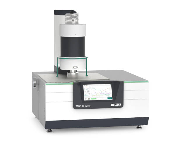
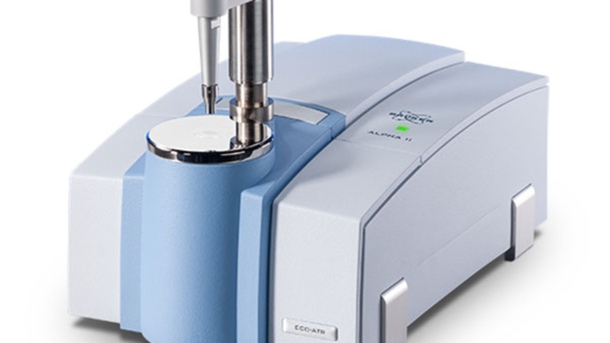
What is FTIR Spectrometer Testing?

Fourier Transform Infrared spectroscopy, commonly known as FTIR, is a chemical analysis technique used to identify materials based on how they absorb infrared radiation. Every material has a unique absorption pattern, often called a fingerprint spectrum.

In simple terms, FTIR testing helps answer one direct question: what is this material made of? This makes it useful for polymer identification, raw material verification, contamination analysis, coating studies, and failure investigation.

Why FTIR Testing is Important

Many product problems begin with wrong material selection, supplier variation, contamination, or chemical mismatch. If you do not verify the material, you are only depending on paperwork or supplier claims. That is weak quality control.

By choosing fourier transform infrared FTIR spectrometer testing in Chennai – Kiyo R&D Center & Laboratory, customers can:

  • Identify unknown materials and residues
  • Verify polymer and rubber composition
  • Compare failed samples with approved samples
  • Detect contamination or foreign substances
  • Support customer complaint and failure analysis
  • Improve incoming material inspection

FTIR is especially useful when fast, practical chemical identification is required before deeper analysis or decision-making.

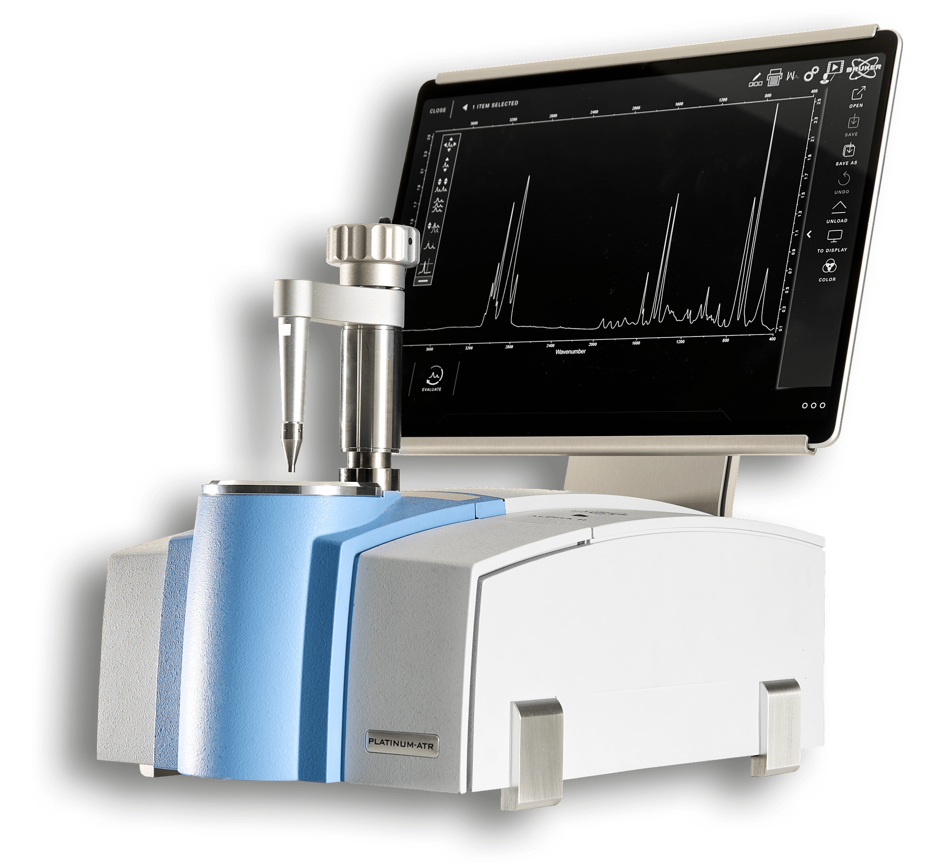
How FTIR Spectrometer Testing Works

FTIR testing works by passing infrared radiation through or across the sample. Different chemical bonds absorb infrared energy at different wavelengths. The instrument records these absorptions and creates a spectrum with characteristic peaks.

The spectrum is then compared with known reference data or a control sample. This helps identify the material type or detect differences between two samples. For example, a good sample and a failed sample can be compared to check whether chemical changes, contamination, or material substitution may have occurred.

Applications of FTIR Testing in Chennai

FTIR is widely used across manufacturing and R&D because it gives fast and useful chemical information. It is commonly used for plastic identification, rubber analysis, adhesive verification, coating analysis, oil and grease residue identification, packaging material study, and foreign particle investigation.

For plastic and polymer industries, FTIR helps identify materials such as PP, PE, PVC, PET, ABS, nylon, polycarbonate, polyurethane, and other polymer families. For coatings and adhesives, it helps compare formulations and check whether an unknown film or residue matches the expected material.

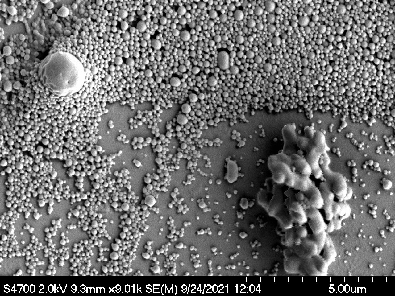
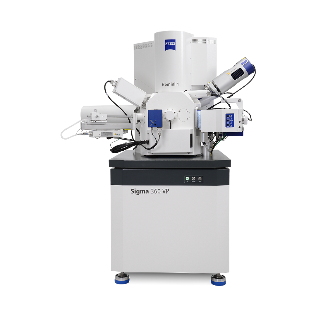
Internal Linking Structure for SEM, TGA and EDAX Pages

To improve SEO strength, this FTIR page should be connected with related material characterization services. Internal links help Google understand that Kiyo R&D Center & Laboratory offers a complete testing and analysis cluster, not just one isolated service.

Use these links naturally inside the blog:
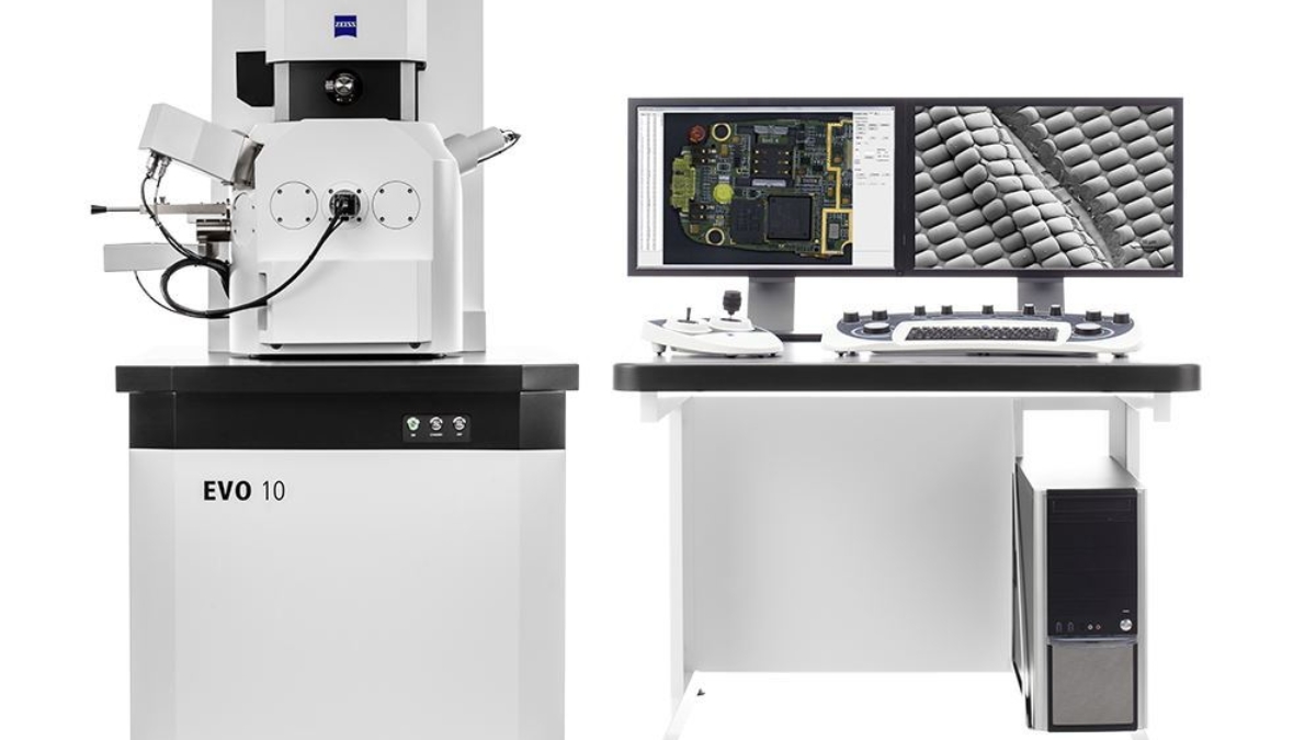
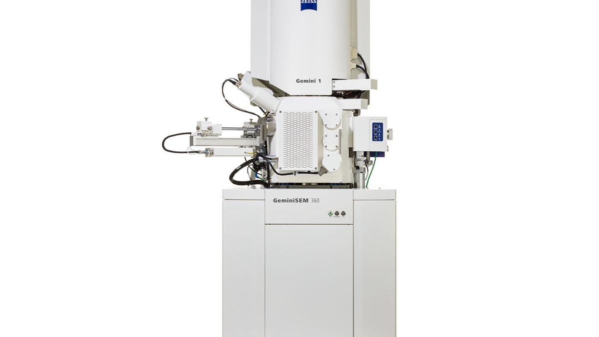
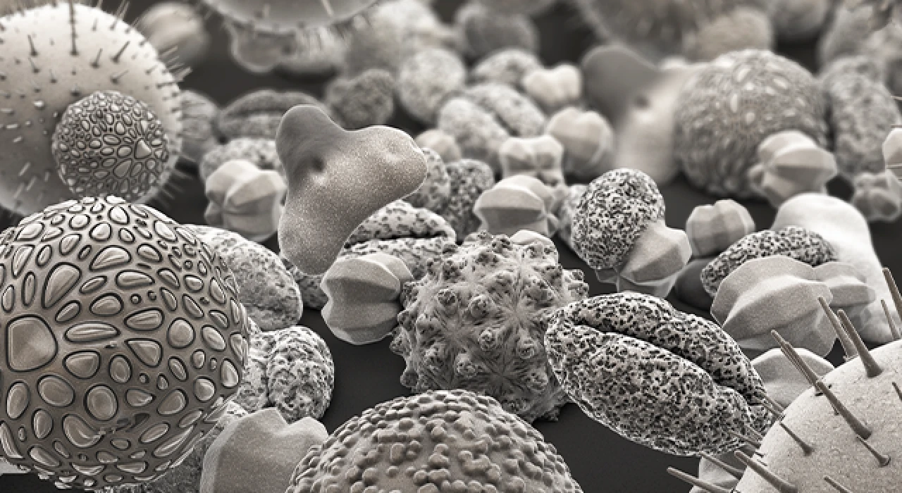
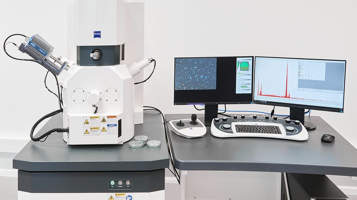
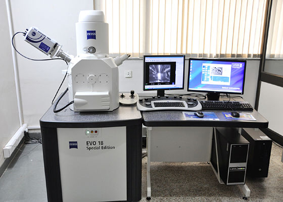
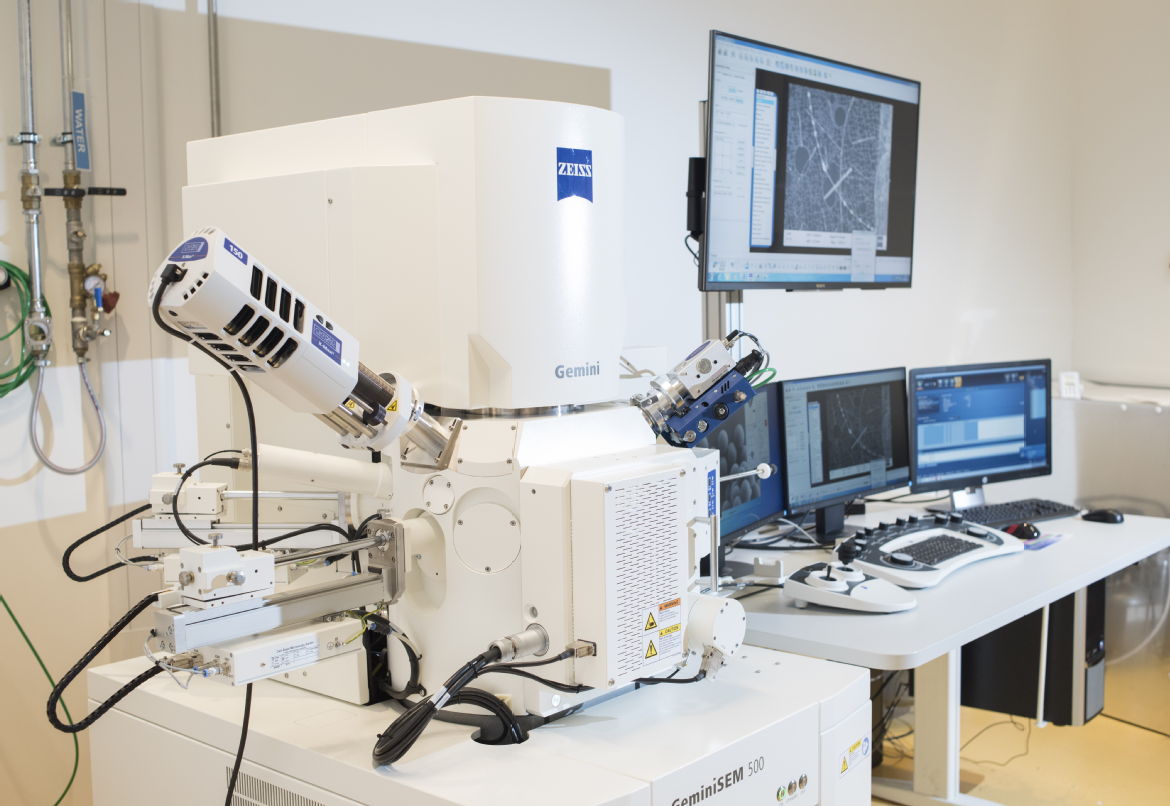
Example: FTIR can identify organic materials such as polymers, adhesives, oils, and coatings. But if the contamination is inorganic or metallic, EDAX analysis may be more useful. If the sample failure involves surface cracks, particles, or fracture features, SEM analysis can support visual investigation. If thermal degradation or filler percentage is suspected, TGA analysis can add stronger evidence.

Why Choose Kiyo R&D Center & Laboratory?

Not every lab gives useful FTIR results. Some labs only provide a spectrum without proper interpretation. That is not enough. A useful FTIR report should help the customer understand what the material likely is and how the result supports the actual problem.

Key advantages of Kiyo R&D Center & Laboratory:
  • FTIR testing for polymers, rubber, coatings, adhesives, residues, and powders
  • Practical interpretation of spectra
  • Comparison of unknown samples with reference materials
  • Support for failure analysis and contamination study
  • Related testing support through SEM, TGA, and EDAX analysis
  • Professional reporting for quality and technical use

The real value is not just identifying peaks. The real value is helping you make the next correct technical decision.

Business Benefits of FTIR Testing

Using fourier transform infrared FTIR spectrometer testing in Chennai – Kiyo R&D Center & Laboratory helps businesses reduce material-related risk. It can prevent wrong material usage, identify contamination early, support supplier quality checks, and help solve customer complaints faster.

FTIR testing is useful for:

  • Incoming raw material verification
  • Product development and formulation comparison
  • Complaint investigation
  • Reverse engineering support
  • Failure analysis
  • Quality control documentation

If your material identity is uncertain, FTIR is often the right starting point.

FTIR Spectrometer Testing in Chennai | Kiyo R&D Center & Laboratory

Work With Kiyo R&D lab

FTIR spectrometer testing is a powerful and practical method for identifying materials and understanding chemical composition. It is especially valuable for polymers, coatings, rubber, adhesives, residues, and unknown substances.

If you are looking for reliable fourier transform infrared FTIR spectrometer testing in Chennai – Kiyo R&D Center & Laboratory, our team can support your requirements with accurate analysis, useful interpretation, and related services such as SEM analysis, TGA analysis, and EDAX analysis.

FAQ

Can FTIR testing identify plastic materials?

Yes. FTIR testing can help identify many common plastic materials such as PP, PE, PVC, PET, ABS, nylon, polycarbonate, polyurethane, and other polymer families by comparing their infrared spectra.

What is the difference between FTIR and EDAX analysis?

FTIR mainly identifies organic chemical bonds and polymer-type materials. EDAX identifies elemental composition such as metals, inorganic particles, and mineral-based contamination. In many failure cases, both tests may be needed.

Can TGA analysis be combined with FTIR testing?

Yes. TGA analysis can support FTIR by showing thermal stability, decomposition behavior, filler content, and weight loss pattern of the material.

How much sample is needed for FTIR testing?

The required sample quantity depends on the material type and testing mode. Usually, FTIR can be performed with a small amount of solid, powder, film, liquid, or residue sample.

Why choose Kiyo R&D Center & Laboratory for FTIR testing in Chennai?

Kiyo R&D Center & Laboratory provides FTIR testing with practical interpretation, professional reporting, and related support through SEM, TGA, and EDAX analysis for deeper material investigation.

EDS Energy Dispersive Spectroscopy Analysis in Oragadam | Kiyo R&D LAB

EDS Energy Dispersive Spectroscopy Analysis in Oragadam | Kiyo R&D LAB

EDS Energy Dispersive Spectroscopy Analysis in Oragadam

Best EDS Analysis Lab in Oragadam for Material Composition | Kiyo R&D LAB

EDS Energy Dispersive Spectroscopy

When a material fails, the real reason is often hidden deep within its composition. Surface-level inspection is not enough. You need to know what elements are present, whether contamination exists, and whether the material matches the expected specification. That is exactly where EDS energy dispersive spectroscopy analysis in Oragadam – Kiyo R&D LAB becomes important.

At Kiyo R&D LAB, we provide advanced elemental analysis support for industries working with metals, polymers, coatings, composites, powders, and engineered materials. Our EDS analysis is commonly used along with SEM imaging to give both surface morphology and elemental composition in one study. For businesses that need real answers instead of guesswork, this service is a practical tool for quality control, failure investigation, and material verification.

EDS Energy Dispersive Spectroscopy Analysis in Oragadam | Kiyo R&D LAB

What is EDS Energy Dispersive Spectroscopy Analysis?

EDS, also called EDX or commonly referred to in industry as EDAX analysis, is a material characterization technique used to identify the elemental composition of a sample. It is usually attached to a scanning electron microscope, where the sample is exposed to an electron beam. The material then emits characteristic X-rays, and those signals are analyzed to determine which elements are present.

In plain language, EDS tells you what your sample is made of at a localized area. That makes it extremely useful when you need to check whether a material contains the right elements, whether unwanted contamination is present, or why a component failed during use.

Why Industries Need EDS Analysis

Too many material decisions are made based on supplier claims, assumptions, or incomplete data. That is careless. If you are serious about product quality, you need proof. With EDS energy dispersive spectroscopy analysis in Oragadam – Kiyo R&D LAB, manufacturers and product developers can verify elemental composition before problems become expensive.

EDS analysis is widely useful for:

  • Identifying unknown particles or residues
  • Investigating material failure and fracture surfaces
  • Checking coating composition
  • Comparing raw materials from different suppliers
  • Detecting contamination in production samples
  • Supporting research and development for new materials

If your component performance depends on composition, skipping elemental analysis is poor practice. You are not saving money. You are increasing risk.

How EDS Analysis Works at Kiyo R&D LAB

The testing process begins with sample review and preparation. Depending on the material type, the sample may be cleaned, mounted, or sectioned to make it suitable for analysis. It is then placed inside the SEM chamber, where the electron beam interacts with the surface. The EDS detector captures X-ray signals and converts them into an elemental spectrum.

Our technical team studies the spectrum, identifies elemental peaks, and interprets the result based on the material and application. If required, elemental mapping can also be used to show where specific elements are distributed across the sample surface. This helps clients understand not just what is present, but where it is present.

Applications of EDS Energy Dispersive Spectroscopy Analysis in Oragadam

EDS analysis is useful across multiple industrial sectors. In automotive and engineering industries, it helps verify alloy composition and identify contaminants in failed parts. In plastics and polymer applications, it helps detect fillers, additives, and foreign particles. In coatings and surface engineering, it supports the study of deposited layers, corrosion products, and coating inconsistencies.

Electronics manufacturers use EDS to analyze solder joints, deposits, and foreign matter on components. Research teams use it for new material development. Quality teams use it to compare batch-to-batch consistency. In every case, the logic is the same: when the composition matters, EDS matters.

Why Choose Kiyo R&D LAB for EDS Analysis in Oragadam?

Choosing a lab is not about picking whoever gives the lowest price. Cheap analysis that leads to wrong interpretation is useless. Kiyo R&D LAB focuses on accuracy, technical clarity, and meaningful reporting.

Our lab supports clients with:

  • Advanced analysis support for metals, plastics, coatings, and composites
  • SEM-linked EDS capability for combined morphology and elemental insight
  • Practical interpretation of results, not just raw spectra
  • Testing support aligned with industrial quality expectations
  • Fast turnaround and professional reporting

This matters because most clients do not just want a graph. They want to know what went wrong, whether the sample passed expectation, and what action to take next.

Internal Linking Structure for Better SEO and Page Authority

To strengthen SEO and improve user navigation, this page should connect naturally with related service pages. Internal links help search engines understand service relationships and keep visitors on the website longer. For this blog, the most relevant internal links are SEM, TGA, and EDAX-related service pages.

You can place internal links like this within the blog or near the conclusion:

These links should not be stuffed randomly. They should appear where they genuinely help the reader understand related services. For example, when explaining surface morphology, link to the SEM page. When discussing elemental analysis with thermal behavior, link to the TGA page. When targeting alternate search habits, link the EDAX page naturally.

EDS Energy Dispersive Spectroscopy Analysis in Oragadam | Kiyo R&D LAB

Work With Kiyo R&D Lab

EDS is one of the most useful tools for material characterization when composition matters. It helps identify elements, detect contamination, support failure analysis, and verify whether a sample meets expectations. For companies that cannot afford wrong assumptions, EDS energy dispersive spectroscopy analysis in Oragadam – Kiyo R&D LAB offers a practical and reliable solution.

Whether you are working on product development, complaint analysis, incoming inspection, or research, Kiyo R&D LAB can support you with clear results and useful technical insight. If you need a deeper study, you can also explore our related services such as SEM analysis, TGA analysis, and SEM with EDAX analysis.

FAQ

Where can I get EDS analysis services in Oragadam for plastics or metal samples?

If you are looking for EDS energy dispersive spectroscopy analysis in Oragadam for plastics, metals, coatings, powders, or composite samples, Kiyo R&D LAB can support elemental analysis requirements with technically relevant reporting.

What is the difference between EDS, EDX, and EDAX analysis?

In practice, these terms are often used interchangeably in industry. EDS and EDX both refer to energy dispersive X-ray-based elemental analysis. EDAX is also widely used as a common market term, although technically it is associated with instrument branding in some contexts.

Can EDS analysis be used for coating and surface layer evaluation?

Yes. EDS is useful for checking coating composition, deposited elements, oxidation products, and localized elemental distribution on surfaces. It can help identify inconsistencies or unwanted material presence.

Can EDS analysis detect all elements in a sample?

EDS can detect many elements, but it has limitations, especially for very light elements and very low concentrations. The suitability depends on the material, detector capability, and analysis objective.

Why should I choose Kiyo R&D LAB for EDS analysis in Oragadam?

Kiyo R&D LAB supports clients with practical elemental analysis, related SEM-based study support, industrial relevance, and professional reporting. The point is not just generating data, but helping clients make better technical decisions.

Flexural Strength Test Services in Oragadam – Accurate Bending Testing | Kiyo R&D LAB

Flexural Strength Test Services in Oragadam – Accurate Bending Testing | Kiyo R&D LAB

Flexural Strength Test Services in Oragadam

ASTM D790 Flexural Testing Services in Oragadam – Kiyo R&D LAB

Flexural Strength Test Services

In real-world applications, materials rarely experience only straight pulling or compression forces. More often, they are subjected to bending loads that can lead to deformation or failure over time. Components such as plastic parts, composite panels, and structural elements are particularly sensitive to bending stress. This is why industries rely on flexural strength test services in Oragadam – Kiyo R&D LAB to evaluate how materials perform under bending conditions.

At Kiyo R&D LAB, flexural strength testing is conducted to measure a material’s ability to resist deformation and fracture when subjected to bending loads. This helps manufacturers ensure that their products will perform reliably in real-world conditions.

Flexural Strength Test Services in Oragadam – Accurate Bending Testing | Kiyo R&D LAB

What is Flexural Strength Testing?

Flexural strength testing measures the maximum stress a material can withstand before it breaks when bent. It is also used to determine stiffness and resistance to deformation.

This type of testing is especially important for materials used in load-bearing applications. Unlike tensile testing, which measures pulling strength, flexural testing focuses on bending behavior, which is often more relevant in practical scenarios.

With flexural strength test services in Oragadam – Kiyo R&D LAB, businesses can accurately evaluate material performance under bending stress.

How Flexural Strength Testing Works

The testing process typically involves placing a sample on two supports and applying a load at the center. This setup is commonly known as a three-point bending test.

As the load increases, the material begins to bend. The test continues until the material either deforms permanently or fractures. The stress at this point is recorded as the flexural strength.

The test also provides additional information such as flexural modulus, which indicates the stiffness of the material, and deflection behavior under load.

At Kiyo R&D LAB, flexural strength test services in Oragadam – Kiyo R&D LAB are performed using calibrated universal testing machines to ensure accurate and repeatable results.

Applications of Flexural Strength Testing

Flexural testing is widely used in industries where materials are subjected to bending forces. In plastic manufacturing, it helps evaluate the performance of molded components. In composite materials, it is used to assess structural strength and durability.

In construction, flexural testing ensures that materials can handle load-bearing applications. In automotive industries, it helps verify the resistance of components to bending and deformation.

This makes flexural strength test services in Oragadam – Kiyo R&D LAB essential for product validation and quality control.

Materials That Can Be Tested

Flexural strength testing can be performed on a wide range of materials including plastics, polymers, composites, ceramics, and certain metals. Each material responds differently to bending, and testing helps determine its suitability for specific applications.

Why Businesses Choose Kiyo R&D LAB

Accurate flexural testing requires proper sample preparation, precise equipment, and controlled testing conditions. Not all laboratories can maintain this level of accuracy.

Kiyo R&D LAB follows ASTM D790 and ISO standards to ensure reliable results. The lab uses calibrated equipment and experienced technicians to deliver accurate and repeatable data.

Clear reporting and fast turnaround time help businesses make informed decisions without delaying production.

Benefits of Flexural Strength Testing

Flexural testing provides valuable insights into material performance. It helps identify weak materials, improve product design, and reduce the risk of failure under bending stress.

It also ensures compliance with industry standards and improves overall product reliability. By using flexural strength test services in Oragadam – Kiyo R&D LAB, businesses can enhance durability and performance.

When Should Flexural Testing Be Performed?

Flexural testing should be conducted during material selection, product development, and quality control. It is also important when changing materials or suppliers and during failure analysis.

Performing testing at the right stage helps prevent issues and ensures consistent product performance.

Why Oragadam is a Key Location for Testing Services

Oragadam is a major industrial hub near Chennai, with strong presence in plastics, automotive, and manufacturing industries. These sectors require materials that can withstand bending forces.

This increases the demand for reliable flexural strength test services in Oragadam – Kiyo R&D LAB to ensure product quality and performance.

Flexural Strength Test Services in Oragadam – Accurate Bending Testing | Kiyo R&D LAB

Work With Kiyo R&D Lab

If your product is exposed to bending loads, flexural strength testing is essential. Choosing flexural strength test services in Oragadam – Kiyo R&D LAB ensures that your materials are tested accurately, helping you deliver durable and reliable products.


FAQ

What is a three-point bending test?

It is a test where a sample is supported at two points and loaded at the center to measure bending strength.

What standards are used for flexural testing?

ASTM D790 and ISO standards are commonly used for flexural strength testing.

Which industries use flexural strength testing?

Plastic, automotive, construction, and manufacturing industries use flexural testing.

Why choose Kiyo R&D LAB?

Kiyo R&D LAB provides accurate testing, advanced equipment, and reliable results with fast reporting.

EDX Analysis Services in Oragadam | Elemental Testing – Kiyo R&D LAB

EDX Analysis Services in Oragadam | Elemental Testing – Kiyo R&D LAB

EDX Analysis Services in Oragadam

EDX Analysis Lab in Oragadam, Chennai | Accurate Elemental Testing

EDX Analysis Services

In modern manufacturing, material quality is everything. Even a small variation in composition can lead to major product failures. This is where EDX analysis services in Oragadam – Kiyo R&D LAB play a crucial role.

EDX (Energy Dispersive X-ray Analysis) helps industries understand exactly what their materials are made of. Whether you are working with metals, polymers, coatings, or electronic components, accurate elemental analysis is essential for maintaining product reliability.

EDX Analysis Services in Oragadam | Elemental Testing – Kiyo R&D LAB

What is EDX Analysis?

EDX analysis is an advanced material characterization technique used to identify the elemental composition of a sample. It works by detecting X-rays emitted from the material when exposed to an electron beam.

In simple terms, EDX tells you:

  • Which elements are present in a material
  • The approximate quantity of each element
  • Whether contamination or impurities exist

This makes EDX analysis services in Oragadam – Kiyo R&D LAB essential for industries that demand high accuracy and quality.

Why EDX Analysis is Important for Industries

Industries in Oragadam operate in a highly competitive environment, especially in automotive, electronics, and manufacturing sectors. A small defect in material composition can lead to product failure, rejection, or customer complaints.

Using EDX analysis services in Oragadam – Kiyo R&D LAB, companies can proactively identify issues before they become costly problems.

  • Ensure raw material quality
  • Verify supplier consistency
  • Reduce product failures
  • Improve overall product performance

If you are only testing after a failure occurs, you are already too late.

Applications of EDX Analysis

EDX analysis is widely used across various industries where material performance is critical.

  • Automotive: Component failure analysis and wear studies
  • Electronics: PCB contamination and solder joint analysis
  • Polymers: Additive and filler identification
  • Metals: Alloy composition verification and corrosion studies
  • Coatings: Layer composition and defect analysis

Ignoring material-level analysis is a mistake that leads to repeated failures and increased costs.

EDX vs Traditional Testing Methods

Traditional testing methods often provide bulk composition data but fail to detect localized variations or contamination.

EDX analysis offers:

  • Micro-level elemental detection
  • Fast and accurate results
  • Localized analysis of specific areas
  • Integration with SEM for detailed insights

This is why industries prefer EDX analysis services in Oragadam – Kiyo R&D LAB over conventional methods.

How EDX Helps in Failure Analysis

Failure analysis is one of the most important applications of EDX testing. When a product fails, the actual cost includes downtime, rework, and loss of customer trust.

With EDX analysis services in Oragadam – Kiyo R&D LAB, companies can:

  • Identify foreign particles or contaminants
  • Detect corrosion-causing elements
  • Verify incorrect material usage
  • Analyze coating failures

This allows businesses to fix the root cause instead of repeating the same mistake.

Why Choose Kiyo R&D LAB in Oragadam

Not all testing labs deliver meaningful insights. Many provide raw data without proper interpretation.

EDX analysis services in Oragadam – Kiyo R&D LAB stand out due to:

  • Advanced EDX instrumentation
  • Integration with SEM for deeper analysis
  • Experienced technical experts
  • Accurate and reliable reports
  • Fast turnaround time

The focus is not just on testing, but on delivering actionable insights that help businesses make better decisions.

EDX Analysis Services in Oragadam | Elemental Testing – Kiyo R&D LAB

Work With Kiyo R&D Lab

Material composition plays a critical role in product performance. Relying on assumptions can lead to costly mistakes.

With EDX analysis services in Oragadam – Kiyo R&D LAB, industries gain precise insights into elemental composition, helping improve quality, reduce failures, and enhance reliability.

Investing in accurate material testing is not an expenseβ€”it is a smart business decision.

FAQ

What is EDX analysis used for?

EDX analysis is used to identify and measure the elemental composition of materials for quality control, failure analysis, and contamination detection.

How fast is EDX testing?

EDX works best for solid materials such as metals, polymers, coatings, and composites.

Can EDX detect contamination?

Yes, EDX can detect even small amounts of contamination or unwanted elements in a material.

Why choose Kiyo R&D LAB?

Kiyo R&D LAB provides accurate testing, expert analysis, and fast turnaround for industrial applications.

EDAX Analysis Services in Oragadam – Accurate Elemental Testing | Kiyo R&D LAB

EDAX Analysis Services in Oragadam – Accurate Elemental Testing | Kiyo R&D LAB

EDAX Analysis Services in Oragadam

EDAX Material Analysis Services in Oragadam – Kiyo R&D LAB

EDAX Analysis Services

In material testing, surface appearance often tells only a small part of the story. Many failures happen because of incorrect composition, contamination, or material inconsistency at a microscopic level. These issues cannot be identified through visual inspection alone. That is why industries rely on edax analysis services in Oragadam – Kiyo R&D LAB to understand the true composition of materials before problems occur.

At Kiyo R&D LAB, EDAX (Energy Dispersive X-ray Analysis) is used to identify and quantify the elements present in a material. This helps manufacturers verify quality, detect impurities, and ensure that materials meet required specifications.

EDAX Analysis Services in Oragadam – Accurate Elemental Testing | Kiyo R&D LAB

What is EDAX Analysis?

EDAX analysis is an advanced technique used to determine the elemental composition of materials. It works by detecting X-rays emitted from a sample when it is exposed to an electron beam.

Each element produces a unique X-ray signal, allowing the system to identify and measure the concentration of elements present in the sample. This makes EDAX a powerful tool for material identification and quality control.

With edax analysis services in Oragadam – Kiyo R&D LAB, businesses can obtain accurate composition data without damaging the material.

How EDAX Analysis Works

The process begins by placing a sample inside an analytical instrument, often combined with a scanning electron microscope. An electron beam is directed onto the sample surface.

This interaction causes the material to emit X-rays. These X-rays are captured and analyzed to determine the elements present in the material.

The result is a spectrum that shows the composition and relative concentration of each element. This data helps in understanding material properties and performance.

Applications of EDAX Analysis

EDAX analysis is widely used in industries where material composition is critical. In metallurgy, it is used to verify alloy composition and detect impurities. In electronics, it helps identify contamination that can affect performance.

In coatings and paints, EDAX is used to analyze elemental distribution and identify defects. In polymers and composites, it helps detect fillers and additives.

This makes edax analysis services in Oragadam – Kiyo R&D LAB essential for quality control, research, and failure analysis.

Materials That Can Be Analyzed

EDAX analysis can be performed on a wide range of materials including metals, alloys, plastics, polymers, ceramics, coatings, and composite materials. Each material can be analyzed to determine its elemental composition and ensure quality standards are met.

Why Businesses Choose Kiyo R&D LAB

Accurate EDAX analysis requires advanced equipment and skilled interpretation of results. Not all laboratories can provide reliable insights.

Kiyo R&D LAB ensures precision by using calibrated instruments, following standardized procedures, and employing experienced analysts. The lab provides clear and detailed reports that help businesses make informed decisions.

Fast turnaround time ensures that testing supports production and development without delays.

Benefits of EDAX Analysis

EDAX analysis provides detailed insights into material composition. It helps identify unknown materials, detect impurities, and verify quality. It also supports failure analysis and improves product reliability.

By using edax analysis services in Oragadam – Kiyo R&D LAB, businesses can reduce risks, improve quality, and ensure consistent performance.

When Should EDAX Analysis Be Used?

EDAX analysis should be used during raw material verification, product development, and quality control. It is also useful for identifying unknown samples and analyzing failures.

Performing EDAX testing at the right stage helps prevent issues before they affect production or product performance.

Why Oragadam is a Key Location for EDAX Testing

Oragadam is a major industrial hub near Chennai, with strong presence in automotive, electronics, and manufacturing industries. These sectors require accurate material analysis to maintain quality and performance.

This increases the demand for reliable edax analysis services in Oragadam – Kiyo R&D LAB to support industrial growth and innovation.

EDAX Analysis Services in Oragadam – Accurate Elemental Testing | Kiyo R&D LAB

Work With Kiyo R&D Lab

If understanding material composition is important for your business, EDAX analysis is essential. Choosing edax analysis services in Oragadam – Kiyo R&D LAB ensures accurate results, improved product quality, and reduced risk of failure.


FAQ

How accurate is EDAX analysis?

It provides highly accurate results when performed using calibrated instruments and proper procedures.

How long does EDAX testing take?

The duration depends on the sample complexity, but results are usually delivered quickly.

When should EDAX testing be performed?

It should be used during development, quality control, failure analysis, and material identification.

Why choose Kiyo R&D LAB?

Why choose Kiyo R&D LAB?
SEM EDX Analysis Services in Oragadam – Advanced Material Testing | Kiyo R&D LAB

SEM EDX Analysis Services in Oragadam – Advanced Material Testing | Kiyo R&D LAB

SEM EDX Analysis Services in Oragadam

SEM with EDX Elemental Analysis Services in Oragadam – Kiyo R&D LAB

Scanning Electron Microscope with Energy Dispersive X-Ray Analysis Services

In advanced material testing, many critical issues are not visible at the surface level. Failures often originate at microscopic or even nanoscopic levels, where small defects, contamination, or compositional variations can lead to major problems. That is why industries rely on scanning electron microscope with energy dispersive x ray analysis services in Oragadam – Kiyo R&D LAB to understand materials in depth.

At Kiyo R&D LAB, SEM (Scanning Electron Microscope) combined with EDX (Energy Dispersive X-ray Analysis) provides detailed insights into both surface structure and elemental composition. This combination allows industries to identify root causes of failures and improve material performance.

SEM EDX Analysis Services in Oragadam – Advanced Material Testing | Kiyo R&D LAB

What is SEM with EDX Analysis?

SEM is a high-resolution imaging technique used to examine the surface of materials. It provides detailed images that reveal micro-level features such as cracks, fractures, and coating defects.

EDX is an analytical technique used alongside SEM to determine the elemental composition of a material. It detects and quantifies the elements present in the sample.

Together, SEM and EDX provide a complete understanding of both structure and composition.

How SEM-EDX Analysis Works

The testing process begins by placing a sample inside the SEM chamber. A focused electron beam scans the surface, producing high-resolution images of the material.

At the same time, X-rays emitted from the sample are analyzed using EDX to determine the elements present. This provides both visual and chemical data in a single analysis.

With scanning electron microscope with energy dispersive x ray analysis services in Oragadam – Kiyo R&D LAB, testing is performed using advanced instruments to ensure accurate and reliable results.

Applications of SEM-EDX Analysis

SEM-EDX analysis is widely used across industries where detailed material analysis is required. In the automotive sector, it helps identify failure points and coating defects. In electronics, it is used to inspect components and detect contamination.

In metallurgy, SEM-EDX is used to study microstructures and analyze alloy composition. In polymers and coatings, it helps evaluate surface properties and identify additives or impurities.

This makes scanning electron microscope with energy dispersive x ray analysis services in Oragadam – Kiyo R&D LAB essential for research, quality control, and failure analysis.

Materials That Can Be Analyzed

SEM-EDX analysis is suitable for a wide range of materials including metals, alloys, plastics, polymers, ceramics, coatings, and composite materials. Each material can be analyzed for both surface structure and elemental composition.

Why Businesses Choose Kiyo R&D LAB

Accurate SEM-EDX analysis requires advanced equipment and expert interpretation. Not all laboratories can deliver reliable insights.

Kiyo R&D LAB ensures precision by using high-quality instruments, following standardized procedures, and employing experienced analysts. The lab provides clear and actionable reports that help businesses understand their materials better.

Fast turnaround time ensures that analysis supports production and decision-making processes without delays.

Benefits of SEM-EDX Analysis

SEM-EDX analysis provides detailed insights into material properties. It helps identify defects, detect contamination, and understand material composition at a microscopic level.

It also supports failure analysis, improves product quality, and helps in selecting the right materials for specific applications. By using scanning electron microscope with energy dispersive x ray analysis services in Oragadam – Kiyo R&D LAB, businesses can reduce risks and improve reliability.

When Should SEM-EDX Analysis Be Used?

SEM-EDX analysis should be used when detailed material understanding is required. It is especially useful during failure analysis, product development, quality control, and when identifying unknown materials or contaminants.

It is also valuable for investigating defects that cannot be detected through conventional testing methods.

Why Oragadam is a Key Location for Advanced Testing

Oragadam is a major industrial hub near Chennai, with strong presence in automotive, electronics, and manufacturing industries. These sectors require advanced material analysis to maintain quality and performance.

This increases the demand for reliable scanning electron microscope with energy dispersive x ray analysis services in Oragadam – Kiyo R&D LAB to support innovation and product development.

SEM EDX Analysis Services in Oragadam – Advanced Material Testing | Kiyo R&D LAB

Work With Kiyo R&D Lab

If detailed material analysis is important for your business, SEM-EDX testing is essential. Choosing scanning electron microscope with energy dispersive x ray analysis services in Oragadam – Kiyo R&D LAB ensures accurate insights, better product quality, and reduced risk of failure.


FAQ

Why is SEM-EDX analysis important?

It helps identify defects, analyze composition, detect contamination, and improve product quality.

Is SEM-EDX testing destructive?

SEM-EDX testing is generally non-destructive, though minimal sample preparation may be required.

How accurate is SEM-EDX analysis?

It provides highly accurate results when performed using calibrated instruments and proper procedures.

Can SEM-EDX detect contamination?

Yes, it can identify impurities and contamination at a microscopic level.

Why choose Kiyo R&D LAB?

Kiyo R&D LAB provides advanced testing, accurate results, and reliable reporting with fast turnaround time.