Material problems are often too small to see with normal inspection. A crack, particle, coating defect, surface damage, or fracture pattern may look simple from outside, but the real cause may be hidden at the microscopic level. This is why electron scanning microscope analysis in Oragadam – Kiyo R&D Center & Laboratory is important for manufacturers, researchers, quality teams, and product development engineers.
Kiyo R&D Center & Laboratory provides advanced SEM analysis support for metals, plastics, polymers, coatings, composites, powders, particles, and failed components. Electron scanning microscope analysis helps customers understand surface morphology, fracture behavior, contamination, particle structure, coating defects, and micro-level material features with high magnification.
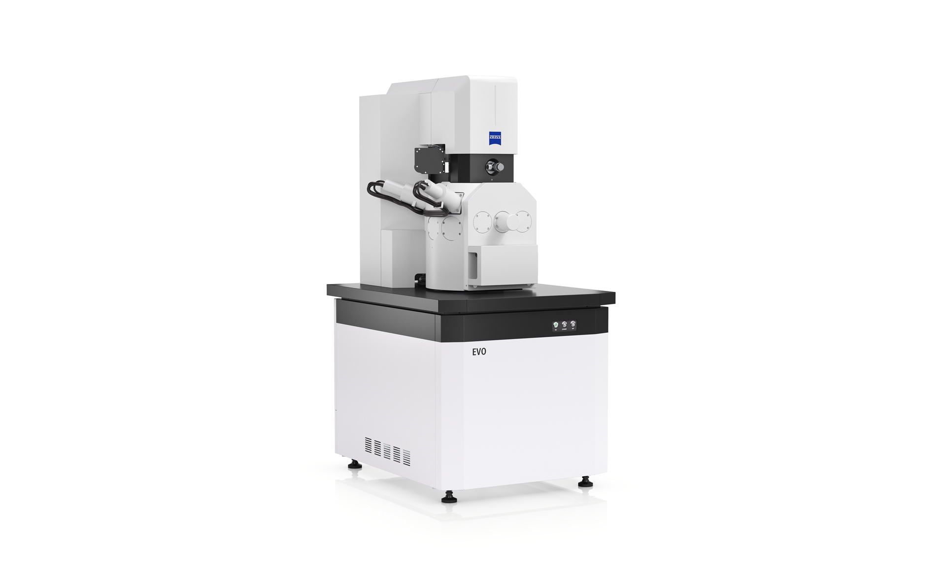
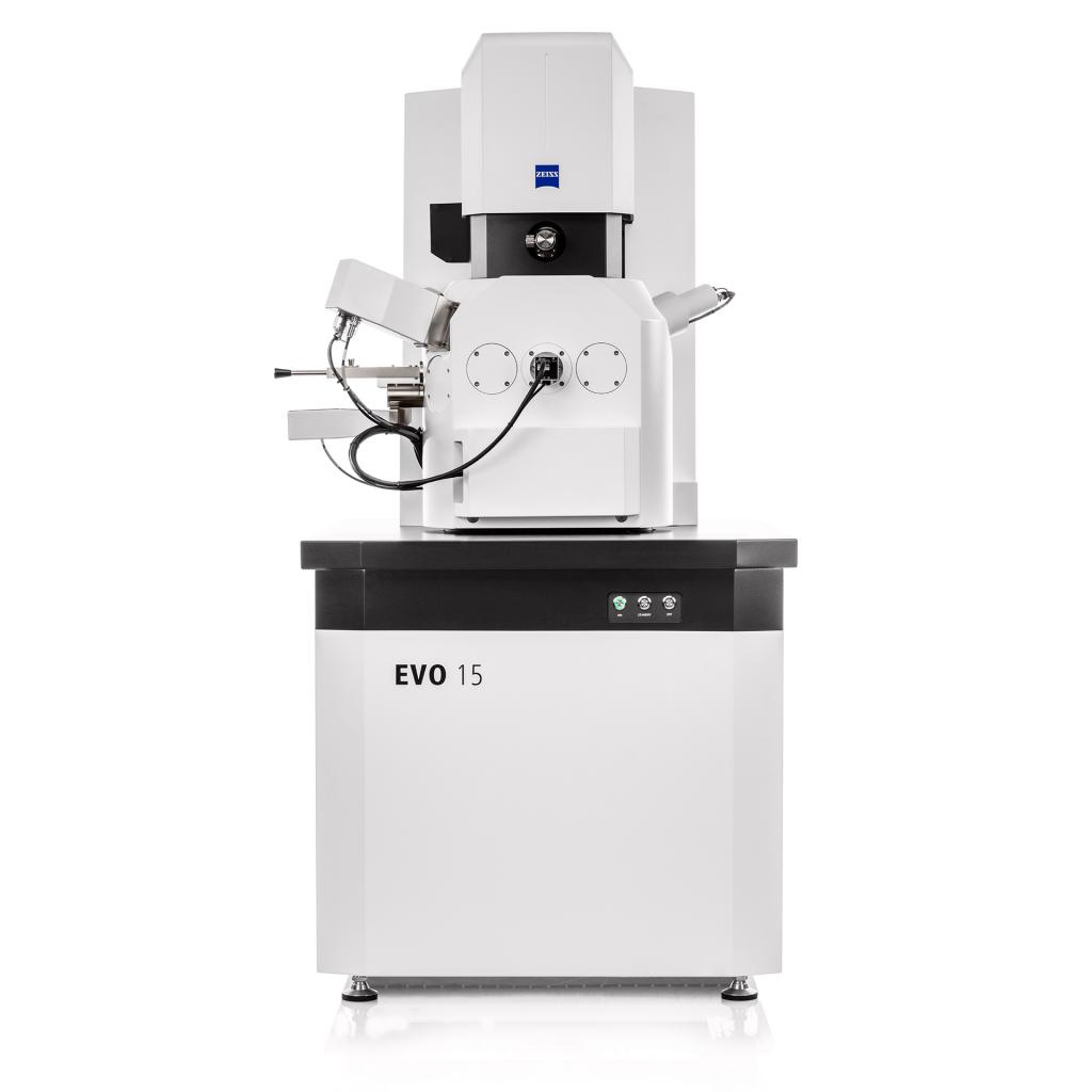
Electron scanning microscope analysis, commonly known as SEM analysis or Scanning Electron Microscopy, is an advanced imaging technique that uses a focused electron beam to scan the sample surface. The result is a high-resolution image that shows surface features in much greater detail than a normal optical microscope.
In simple terms, SEM helps you see what the naked eye cannot see. It is useful when the problem is related to micro-cracks, fracture surfaces, pores, particles, surface roughness, contamination, wear, corrosion, or coating failure.
Trying to solve a material failure without microscopic evidence is poor technical decision-making. Many failures are caused by defects that are not visible during routine inspection. SEM analysis gives visual proof and helps reduce assumptions.
By choosing electron scanning microscope analysis in Oragadam – Kiyo R&D Center & Laboratory, customers can:
The process begins with sample review and preparation. Depending on the material, the sample may need cleaning, drying, cutting, mounting, or conductive coating. The prepared sample is placed inside the SEM chamber, where a focused electron beam scans the surface.
Signals generated from the sample are captured and converted into detailed images. These images are then interpreted to understand surface condition, fracture features, particle shape, coating behavior, or defect morphology. If elemental composition is required, SEM can be combined with EDAX or EDS analysis.
SEM analysis is useful across industries where material quality and failure prevention matter. It is commonly used for fracture analysis, powder morphology, surface contamination, coating defects, corrosion study, wear analysis, polymer failure, composite failure, and microstructure observation.
For plastics and polymers, SEM can reveal fracture surfaces, filler dispersion, voids, and surface defects. For metals, it can show corrosion products, fatigue features, wear tracks, and fracture patterns. For coatings, it helps identify cracks, peeling, roughness, and layer-related defects.
SEM gives detailed images, but sometimes imaging alone is not enough. Customers may also need to know what elements are present in a selected area. In such cases, SEM with EDAX, EDS, or EDX analysis is useful.
SEM with EDAX analysis can help identify foreign particles, contamination, coating elements, fillers, corrosion products, and deposits. For example, if an unknown particle is found on a failed component, SEM can show its shape and size, while EDAX can identify its elemental composition.
A clear SEM image is useful only when it is interpreted properly. Some labs provide images but no meaningful explanation. That is not enough for client decision-making. Kiyo R&D Center & Laboratory focuses on image quality, technical interpretation, and practical reporting.
Electron scanning microscope analysis is a powerful tool for understanding material behavior at the micro level. It helps reveal surface damage, fracture features, contamination, particles, coating defects, and structural details that cannot be seen by normal inspection.
If you are looking for reliable electron scanning microscope analysis in Oragadam – Kiyo R&D Center & Laboratory, our team can support your requirements with high-resolution SEM imaging, useful interpretation, SEM-EDAX support, and professional reporting.
Electron scanning microscope analysis is used to study surface morphology, fracture surfaces, cracks, pores, coating defects, corrosion, wear marks, particle shape, powder structure, and micro-level material defects.
Yes. SEM analysis can be used for plastic and polymer samples to study fracture behavior, surface defects, filler distribution, voids, cracks, and failure features.
SEM analysis shows high-resolution surface images. EDAX analysis identifies the elements present in selected areas. SEM tells you what the surface looks like, while EDAX helps tell what it is made of.
Sample requirement depends on the material type, size, shape, and analysis objective. Small pieces, powders, films, coatings, particles, or failed fragments can usually be evaluated after proper preparation.
Clients should choose Kiyo R&D Center & Laboratory because the lab provides high-resolution SEM imaging, practical interpretation, SEM-EDAX support, and professional reporting that helps customers understand defects and make better technical decisions.
We specialize in material and product testing, providing tailored solutions to meet each client’s unique needs.
For quotation or visit