SEM and EDS Analysis Lab in India
Revealing the Invisible: How SEM & EDS Analysis is Revolutionizing Material Testing in India
Introduction
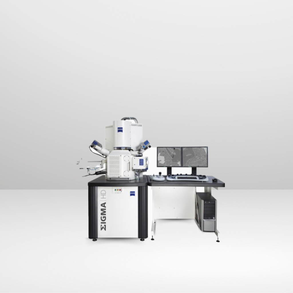
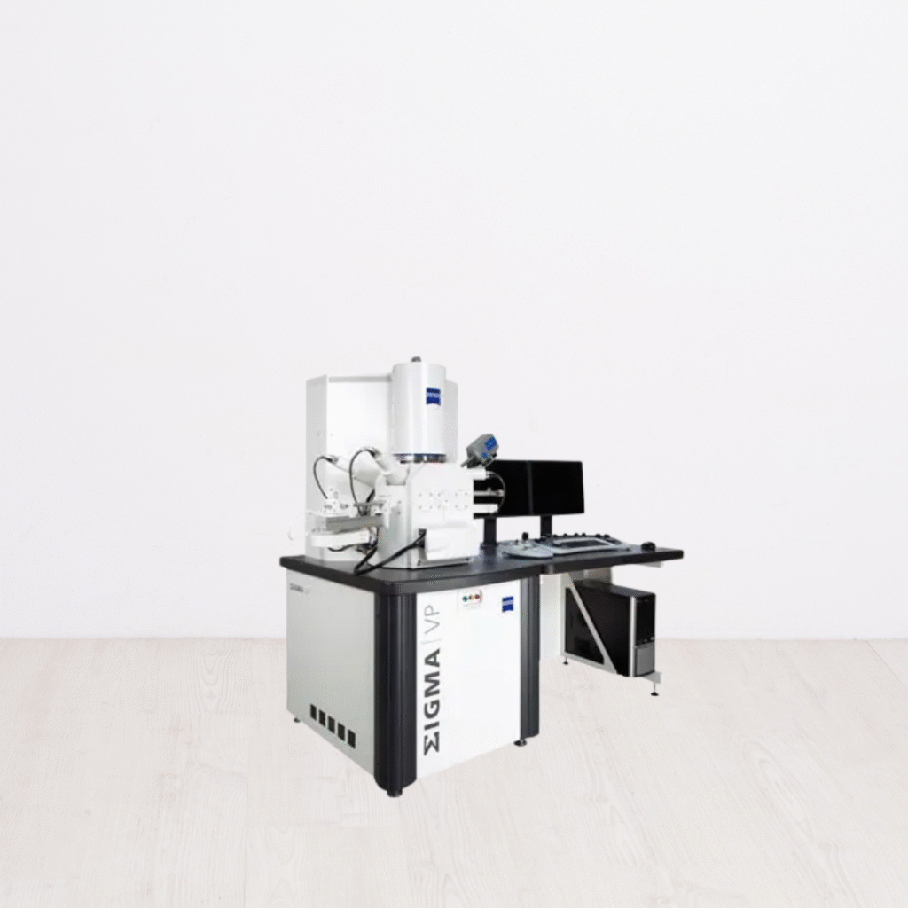
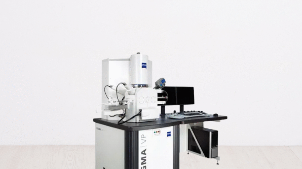
- In today's highly competitive and quality-driven industries, having an in-depth understanding of material properties is not just an advantage—it's essential. This is where SEM (Scanning Electron Microscopy) and EDS (Energy Dispersive X-ray Spectroscopy) come into play. At Kiyo R&D Center & Laboratory, we are proud to offer advanced SEM and EDS analysis services that provide deep insights into a material’s microstructure and elemental composition.

Seeing Beyond the Surface with SEM
Conventional testing methods can only go so far. When your product’s performance depends on microscopic or nanoscopic characteristics, SEM is your answer. By using a focused beam of electrons, SEM creates detailed images of a material’s surface—revealing cracks, defects, phase boundaries, and surface treatments that are otherwise invisible.
Whether you’re developing a new polymer blend, examining a failure point in a metal component, or validating a coating process, SEM imaging gives you the data you need to make informed decisions.
EDS: Unlocking Elemental Clarity
Pairing SEM with EDS analysis gives an added layer of insight. EDS identifies the elemental composition of the materials being scanned, highlighting variations, contaminants, and material mismatches at a microscopic scale.
This is especially valuable in:
Contamination analysis
Alloy verification
Coating and plating thickness inspection
Composite material evaluation
Why Industries Choose Kiyo R&D for SEM and EDS Testing
At Kiyo R&D Center & Laboratory, our mission is to provide clients with accurate, actionable data using world-class instruments and technical expertise. Here’s why clients across India rely on us:
⚙️ State-of-the-Art Equipment – High-resolution SEM with integrated EDS capabilities.
🧪 Cross-Industry Expertise – Trusted by manufacturers in automotive, aerospace, polymers, and electronics.
⏱️ Fast Turnaround Times – Efficient processing to keep your projects on schedule.
📈 Research-Focused Reporting – Detailed, easy-to-understand analysis backed by scientific insight.
Real-World Applications
From R&D to failure analysis and quality control, SEM and EDS analysis play a pivotal role across multiple sectors:
Diagnosing failure in critical machine parts
Ensuring purity in food-contact plastics
Investigating wear patterns in coatings
Studying filler dispersion in composites
Whatever the need, SEM and EDS help turn invisible issues into clear solutions.

Partner with Kiyo R&D Today
- With our laboratory based in India, we provide easy access to advanced materials testing without compromising on quality. Our expert team ensures that every report delivers value—whether you're solving problems or innovating new solutions.

