Your complete guide to ASTM E986 at Kiyo R&D Lab
How sharp is your SEM’s electron beam, really? That single answer decides the finest detail your images can resolve — and it’s exactly what astm e986 sets out to measure. This standard practice describes how to characterize the effective beam size of a scanning electron microscope, giving labs a consistent, repeatable way to check imaging performance.
Whether you’re qualifying an instrument, troubleshooting soft images, or making sure your composition work rests on sound imaging, this practice matters. At Kiyo R&D Lab we apply this discipline so our SEM and SEM-EDX results stay accurate and defensible. Below, we break down what it covers, why it’s used, and how it supports reliable microscopy.
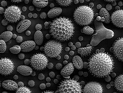
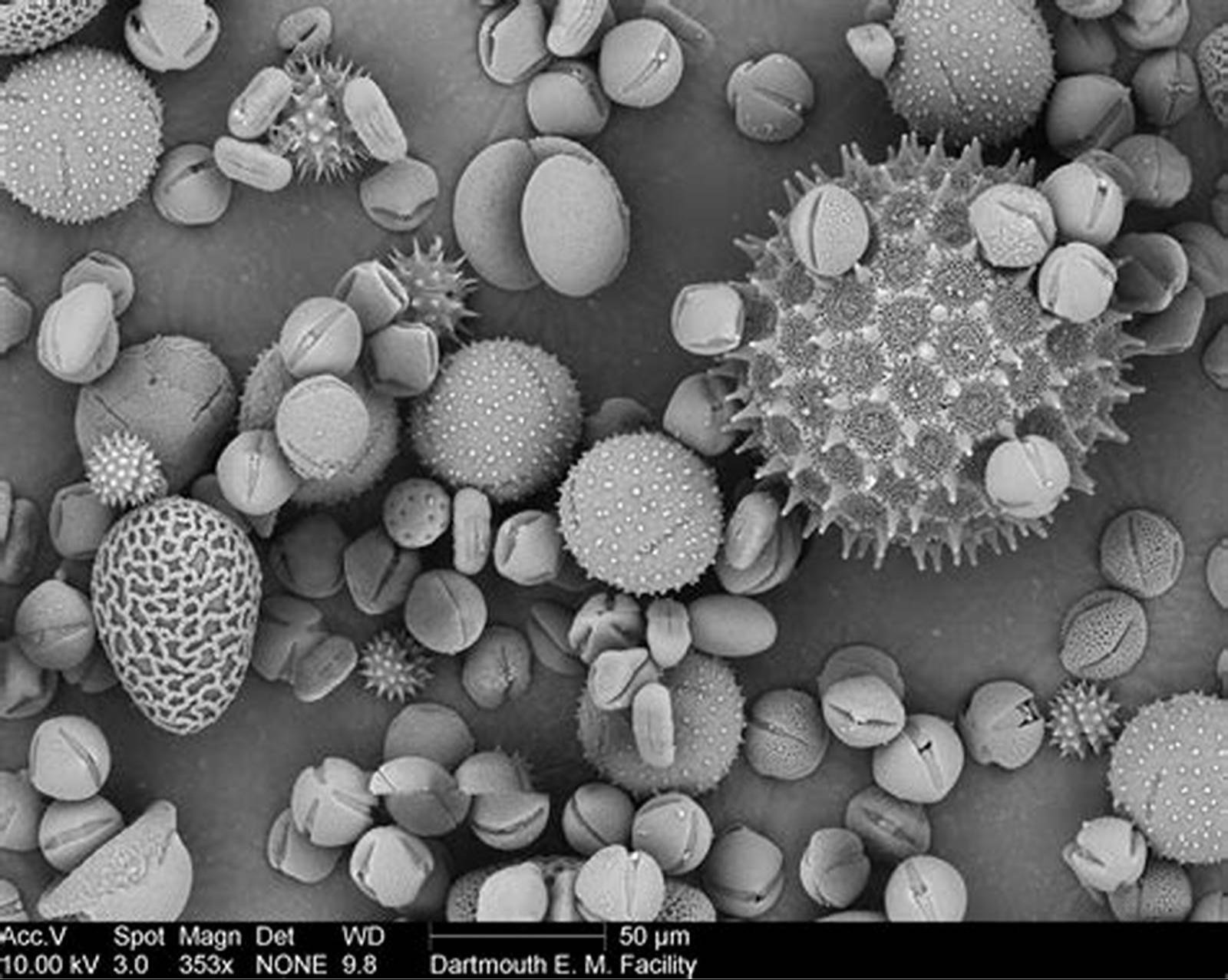
ASTM E986 is a standard practice that describes how to characterize the effective electron-beam size of a scanning electron microscope. The beam is the focused spot of electrons the SEM scans across a sample; its size largely determines the smallest feature the instrument can resolve. By defining a consistent method to measure that spot, this standard practice lets different operators and labs describe SEM imaging performance in comparable terms.
In short, it answers a practical question: is the microscope performing to the resolution you expect? That underpins everything from sharp imaging to reliable elemental analysis performed at the same spot.
The practice behind E986 involves imaging a suitable sharp-edged or fine reference feature and analysing how the signal changes across that edge. The sharper the transition, the smaller the effective beam — and the finer the detail the SEM can resolve.
Confirms finest detail resolvable.
Verify a new or serviced SEM.
Diagnose soft or blurry images.
Compare performance consistently.
Sound imaging behind composition.
Documented, defensible imaging.
| Aspect | What It Describes | Impact |
|---|---|---|
| Effective beam size | Spot diameter on sample | Finer = higher resolution |
| Edge sharpness | Signal change across an edge | Basis of the measurement |
| Focus & astigmatism | Beam shape & tuning | Affects apparent size |
| Operating settings | kV, working distance | Change beam behaviour |
In practice, this SEM beam-size standard sits alongside other standards that govern SEM imaging and EDS composition, so a complete analysis is fully documented.
ASTM ISO
| Standard | What It Covers | Area |
|---|---|---|
| ASTM E986 | SEM beam size characterization | Imaging |
| ISO 16700 | SEM magnification calibration | Imaging |
| ASTM E1508 | Quantitative analysis by EDS | Composition |
| ISO 22309 | Quantitative EDS analysis | Composition |
Together, beam characterization, magnification calibration, and EDS methods make SEM-EDX results both sharp and quantitatively sound.
Based in Chennai with branches in Chrompet and Oragadam, Kiyo R&D Lab applies sound imaging discipline — including the principles behind this SEM beam standard — to our SEM and SEM-EDX work, so your images and elemental data are reliable and well-documented.
Need SEM imaging or SEM-EDX composition analysis you can trust? Our team delivers sharp imaging and reliable elemental data with clear reporting.
📞 Call 90420 86986 💬 Request a QuoteExplore all our capabilities at www.kiyorndlab.com.
Good microscopy starts with a well-characterized beam. The discipline behind astm e986 is what keeps SEM imaging sharp and comparable — and it’s the foundation for trustworthy SEM-EDX composition work. At Kiyo R&D Lab, we bring that rigour to every analysis.
Whether you need SEM imaging, elemental analysis, or guidance on the right approach, our team is ready to help. Reach out today and get results you can stand behind.
We specialize in material and product testing, providing tailored solutions to meet each client’s unique needs.
For quotation or visit