Material problems are not always visible on the surface. A plastic part may crack because of poor bonding, a metal component may fail due to micro-level defects, or a coating may peel because of poor surface structure. Normal visual inspection cannot reveal these details. This is why scanning electron microscopy analysis in Oragadam – Kiyo R&D Center & Laboratory is important for industries that need accurate material investigation.
Kiyo R&D Center & Laboratory provides SEM analysis support for metals, plastics, polymers, composites, coatings, powders, particles, and failed components. SEM helps customers see surface morphology, fracture features, particle shapes, coating defects, and microstructural details with high magnification and clarity.

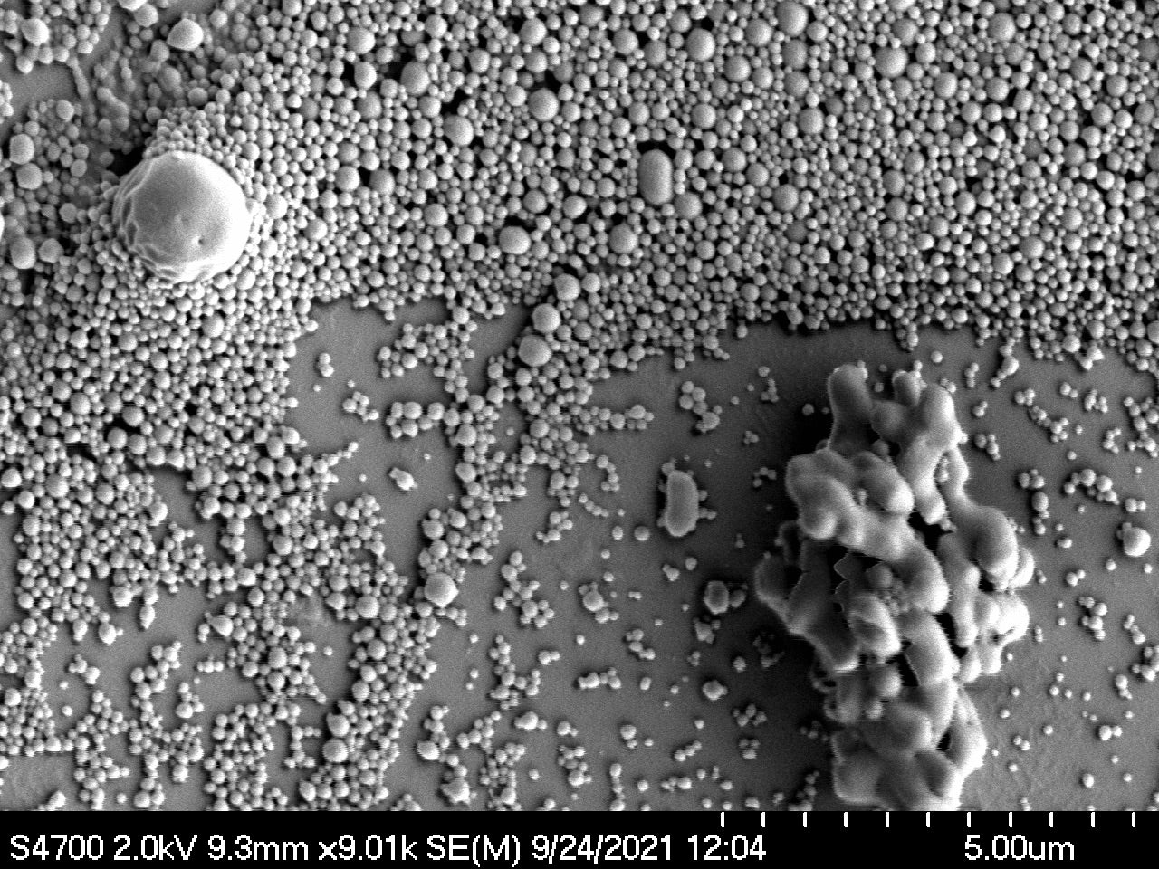
Scanning Electron Microscopy, commonly called SEM, is an advanced imaging technique used to study material surfaces at very high magnification. Instead of using visible light like a normal microscope, SEM uses a focused electron beam to scan the sample surface and generate detailed images.
In simple terms, SEM analysis helps you see what cannot be seen with the naked eye or ordinary optical microscopes. It is especially useful when the issue is related to surface damage, fracture behavior, contamination, particle structure, or micro-level defects.
Trying to solve a material failure without microscopic evidence is weak problem-solving. Many failures happen because of defects that are too small to see directly. SEM gives visual proof and helps reduce guesswork.
By choosing scanning electron microscopy analysis in Oragadam – Kiyo R&D Center & Laboratory, customers can:
The SEM analysis process starts with sample review and preparation. Depending on the material, the sample may need cleaning, drying, cutting, mounting, or coating. Once prepared, the sample is placed inside the SEM chamber. A focused electron beam scans the surface, and the emitted signals are used to generate high-resolution images.
The images are then studied to understand surface texture, fracture pattern, particle distribution, coating condition, or defect morphology. If elemental composition is also required, SEM can be combined with EDAX/EDS analysis.
SEM is widely used across industrial and research applications. In failure analysis, it helps identify fracture patterns, fatigue features, brittle failure, ductile tearing, and surface damage. In powders and particles, it helps observe shape, size, agglomeration, and distribution.
For coatings, SEM can reveal cracks, delamination, surface roughness, and layer defects. For polymers and plastics, it can support fracture investigation, filler distribution study, and surface defect analysis. For metals, it helps observe corrosion, wear, microstructural features, and failure surfaces.
SEM gives high-resolution images, but sometimes imaging alone is not enough. You may also need to know what elements are present in a specific area. That is where EDAX, EDS, or EDX analysis becomes useful.
SEM with EDAX analysis can help identify contamination, foreign particles, coating elements, corrosion products, fillers, and deposits. For example, if a failed part has unknown particles on the surface, SEM can show the particle shape while EDAX can identify the elemental composition.
Not every SEM image is useful. A clear image without correct interpretation can still lead to wrong decisions. Kiyo R&D Center & Laboratory focuses on proper imaging, application understanding, and practical reporting.
The goal is simple: help customers see the problem clearly and make better technical decisions.
Scanning Electron Microscopy is one of the most powerful tools for surface and microstructure analysis. It helps industries investigate failures, study defects, observe particles, and understand material behavior at high magnification.
If you are looking for reliable scanning electron microscopy analysis in Oragadam – Kiyo R&D Center & Laboratory, our team can support your requirements with high-resolution imaging, technical interpretation, and related SEM-EDAX analysis support.
You can get scanning electron microscopy analysis in Oragadam at Kiyo R&D Center & Laboratory for metals, plastics, polymers, coatings, composites, powders, particles, and failed components.
SEM analysis is used to study surface morphology, fracture features, cracks, pores, coating defects, particle shape, powder structure, corrosion damage, wear patterns, and micro-level material defects.
A normal microscope uses visible light and has limited magnification. SEM uses an electron beam and provides much higher magnification, better depth of field, and detailed surface imaging.
Yes. SEM is useful for powder and particle analysis because it can show particle shape, size, surface texture, agglomeration, and distribution. This is useful in materials, coatings, pharmaceuticals, and research applications.
Choose SEM analysis when you need to observe surface features, cracks, particles, or fracture morphology. Choose EDAX analysis when you need elemental composition, contamination identification, or foreign particle analysis. Many cases need both.
Kiyo R&D Center & Laboratory provides SEM analysis with high-resolution imaging, practical interpretation, SEM-EDAX support, and professional reporting for quality control, failure investigation, and research applications.
We specialize in material and product testing, providing tailored solutions to meet each client’s unique needs.
For quotation or visit