In advanced material testing, many critical issues are not visible at the surface level. Failures often originate at microscopic or even nanoscopic levels, where small defects, contamination, or compositional variations can lead to major problems. That is why industries rely on scanning electron microscope with energy dispersive x ray analysis services in Oragadam – Kiyo R&D LAB to understand materials in depth.
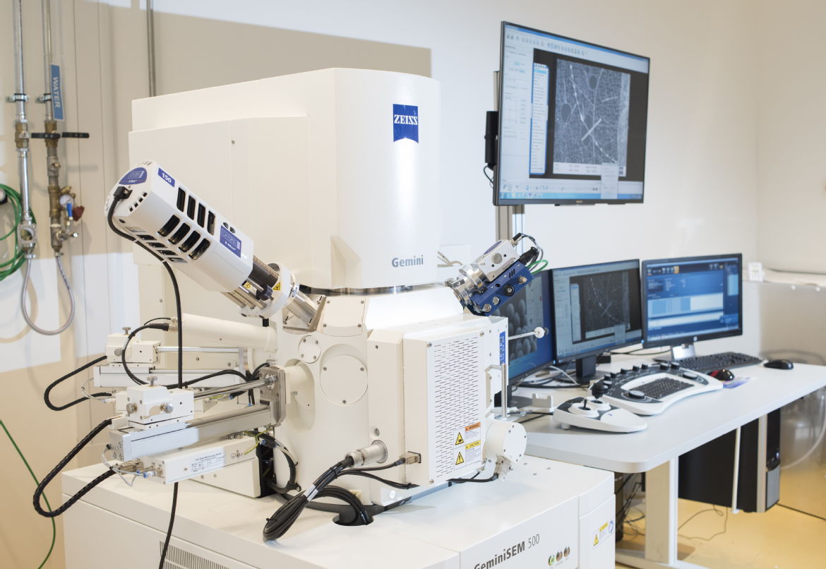
At Kiyo R&D LAB, SEM (Scanning Electron Microscope) combined with EDX (Energy Dispersive X-ray Analysis) provides detailed insights into both surface structure and elemental composition. This combination allows industries to identify root causes of failures and improve material performance.
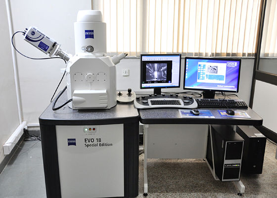
SEM is a high-resolution imaging technique used to examine the surface of materials. It provides detailed images that reveal micro-level features such as cracks, fractures, and coating defects.
EDX is an analytical technique used alongside SEM to determine the elemental composition of a material. It detects and quantifies the elements present in the sample.
Together, SEM and EDX provide a complete understanding of both structure and composition.
The testing process begins by placing a sample inside the SEM chamber. A focused electron beam scans the surface, producing high-resolution images of the material.
At the same time, X-rays emitted from the sample are analyzed using EDX to determine the elements present. This provides both visual and chemical data in a single analysis.
With scanning electron microscope with energy dispersive x ray analysis services in Oragadam – Kiyo R&D LAB, testing is performed using advanced instruments to ensure accurate and reliable results.
SEM-EDX analysis is widely used across industries where detailed material analysis is required. In the automotive sector, it helps identify failure points and coating defects. In electronics, it is used to inspect components and detect contamination.
In metallurgy, SEM-EDX is used to study microstructures and analyze alloy composition. In polymers and coatings, it helps evaluate surface properties and identify additives or impurities.
This makes scanning electron microscope with energy dispersive x ray analysis services in Oragadam – Kiyo R&D LAB essential for research, quality control, and failure analysis.
SEM-EDX analysis is suitable for a wide range of materials including metals, alloys, plastics, polymers, ceramics, coatings, and composite materials. Each material can be analyzed for both surface structure and elemental composition.
Accurate SEM-EDX analysis requires advanced equipment and expert interpretation. Not all laboratories can deliver reliable insights.
Kiyo R&D LAB ensures precision by using high-quality instruments, following standardized procedures, and employing experienced analysts. The lab provides clear and actionable reports that help businesses understand their materials better.
Fast turnaround time ensures that analysis supports production and decision-making processes without delays.
SEM-EDX analysis provides detailed insights into material properties. It helps identify defects, detect contamination, and understand material composition at a microscopic level.
It also supports failure analysis, improves product quality, and helps in selecting the right materials for specific applications. By using scanning electron microscope with energy dispersive x ray analysis services in Oragadam – Kiyo R&D LAB, businesses can reduce risks and improve reliability.
SEM-EDX analysis should be used when detailed material understanding is required. It is especially useful during failure analysis, product development, quality control, and when identifying unknown materials or contaminants.
It is also valuable for investigating defects that cannot be detected through conventional testing methods.
Oragadam is a major industrial hub near Chennai, with strong presence in automotive, electronics, and manufacturing industries. These sectors require advanced material analysis to maintain quality and performance.
This increases the demand for reliable scanning electron microscope with energy dispersive x ray analysis services in Oragadam – Kiyo R&D LAB to support innovation and product development.
If detailed material analysis is important for your business, SEM-EDX testing is essential. Choosing scanning electron microscope with energy dispersive x ray analysis services in Oragadam – Kiyo R&D LAB ensures accurate insights, better product quality, and reduced risk of failure.
It helps identify defects, analyze composition, detect contamination, and improve product quality.
SEM-EDX testing is generally non-destructive, though minimal sample preparation may be required.
It provides highly accurate results when performed using calibrated instruments and proper procedures.
Yes, it can identify impurities and contamination at a microscopic level.
Kiyo R&D LAB provides advanced testing, accurate results, and reliable reporting with fast turnaround time.
We specialize in material and product testing, providing tailored solutions to meet each client’s unique needs.
For quotation or visit